SR Latches
02 Mar 2019, Ryan JacobsLogic will get you from A to B. Imagination will take you everywhere. — A.E.
We’re going to discuss the building blocks of digital logic in these upcoming guides. It’s good to get the foundations laid down before we advance to the more complicated topics.
Everything in sequential logic is dependent on state. State is the driving component that gives value to most systems. (Pattern recognizers, neural networks, video processors, networking routers, caches, etc.) And the key to creating state is the flip-fop. The flip-flop can hold state; it can remember. On or off. 1 or 0. It’s a crucial piece of the digital logic puzzle.
What’s a Flip-Flop?
No, it’s not a sandal.
Before we can understand flip-flops, we need to understand latches. So get on your binary boots and let’s dive in.
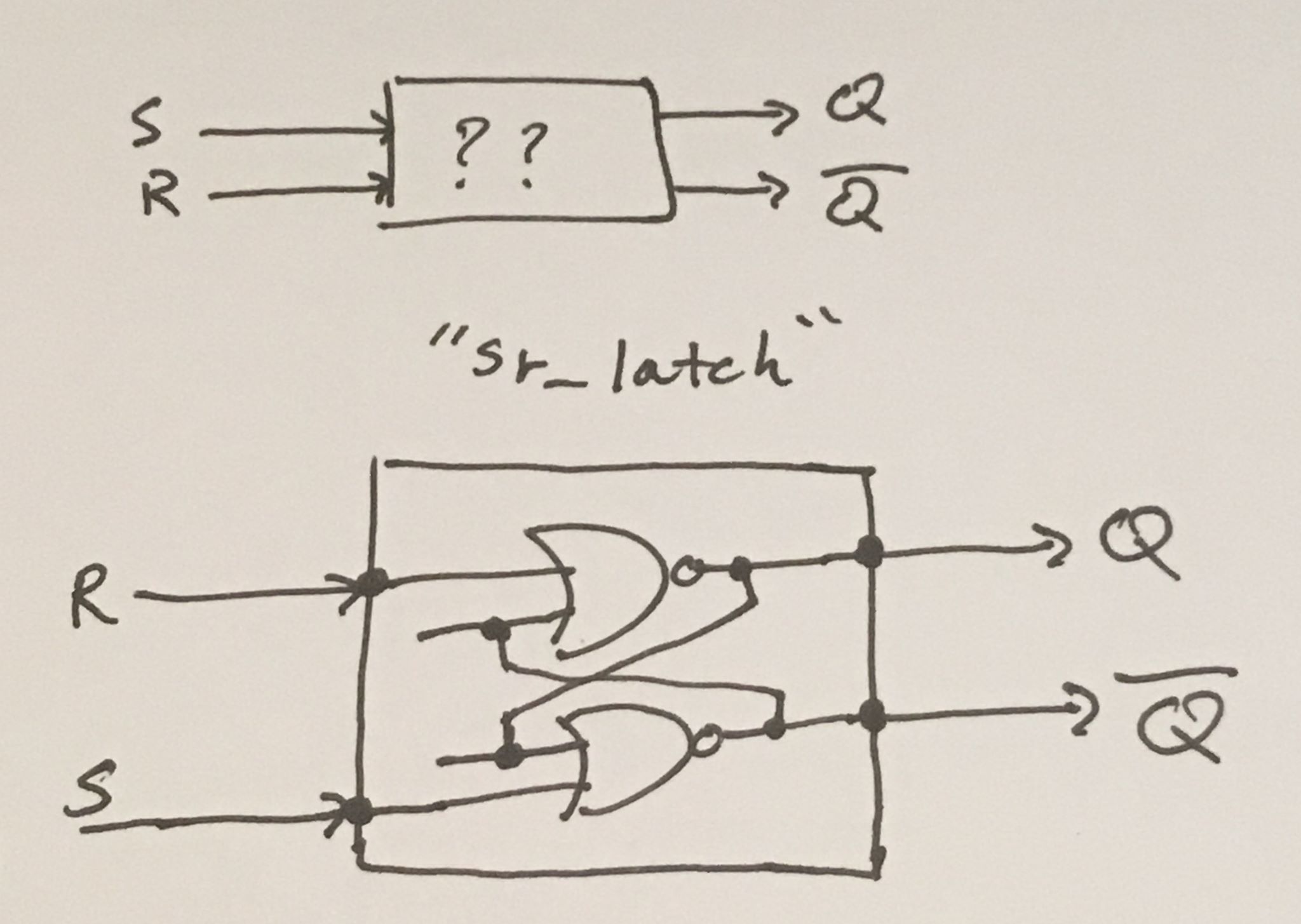
Intro to Latches
a.k.a. “bistable multivibrators”
Wow, jeez that sounds complicated doesn’t it? But don’t fret, I’ll break down those high-syllable words for you.
bistable means that the device has two states (hence “bi”) and will eventually settle one state that remains stable — once the system has reached equilibrium, that is no oscillation, no vibration. In other words, these devices have the unique ability to receive inputs at one time, settle on a state, and then recite that that state at a later point in time.
Latches are the basic building blocks required to store state. They are a crucial tool that allows our logic designs to possess memory. Without the ability to remember states, most systems would be completely useless. Imagine if your processor had no registers. It would be incapable of functioning at all, no stack pointers, no cache, nil.
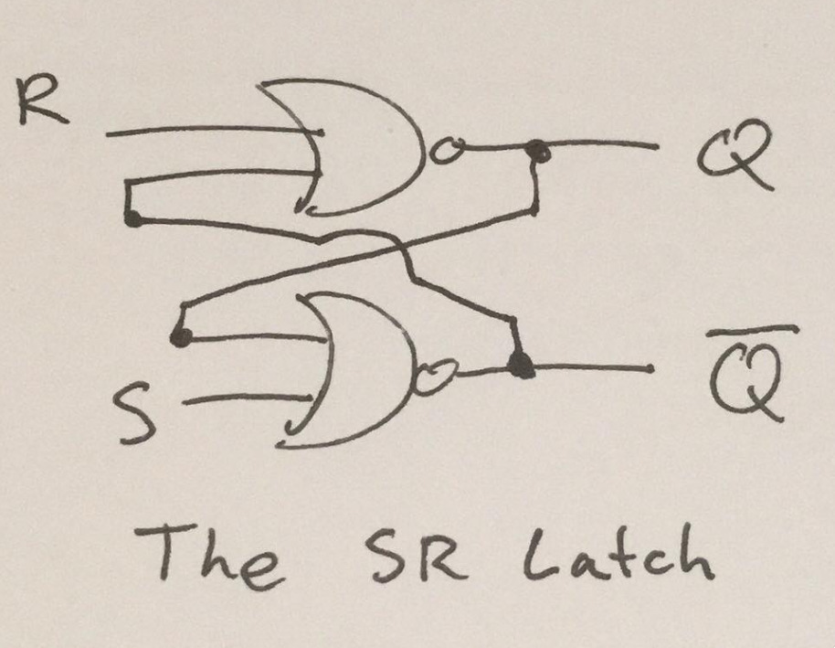
How a Latch Works
To create one for ourselves, we can cross-couple two NOR gates. In other words, we connect them in a way such that the output of one feeds into the input of the other and vice versa.
Here’s how it’s drawn:
 There are other methods to create an SR
Latch (such as with NAND gates), however NOR gates are the most intuitive,
so we'll stick with them.
There are other methods to create an SR
Latch (such as with NAND gates), however NOR gates are the most intuitive,
so we'll stick with them.
(Normally I'd steal a nice vector diagram off the web, but apparently that's frowned upon by the people I take it from. So I apologize if my drawings are amateur.)
And it’s truth table:
| S | R | Q | ~Q | effect |
|---|---|---|---|---|
| 0 | 0 | Q(t-1) | ~Q(t-1) | latch |
| 0 | 1 | 0 | 1 | reset |
| 1 | 0 | 1 | 0 | set |
| 1 | 1 | 0 | 0 | invalid/illegal |
It’s not difficult to see the use cases when the table is laid out in this way.
S and R are the inputs to the latch, and they produce an effect on Q and ~Q.
(By definition, ~Q will always be opposite of Q.) When changing or setting
state, we always set S and R to opposite values. We set S to 1 when we
want Q to be 1 (the set effect). We set S to 0 when we want Q to be 0
(the reset effect). Keeping S and R both at 0, will leave the state
alone — this is called the latch effect. The notation of Q being
equal to Q(t-1) simply means that Q will maintain its previous state,
whatever it may have been.
At this point, your eyes might have glazed over. That’s definitely okay. The rest of this section will go into more detail on how all the pieces interact together on a lower level. This should help your understanding.
Personally, I couldn’t see how latches actually did their magic until I drew
it out. Maybe you’re the same way. There’s only four cases, so it’s not awfully
difficult check yourself. But we’ll do one right now. We’ll test the set
effect by setting S to 1 and R to 0.
Also, just for reference: an OR gate will output a 1 if either input is a 1,
otherwise 0. So it would follow that a NOR gate will output a 0 if
either input is a 1, otherwise 1.
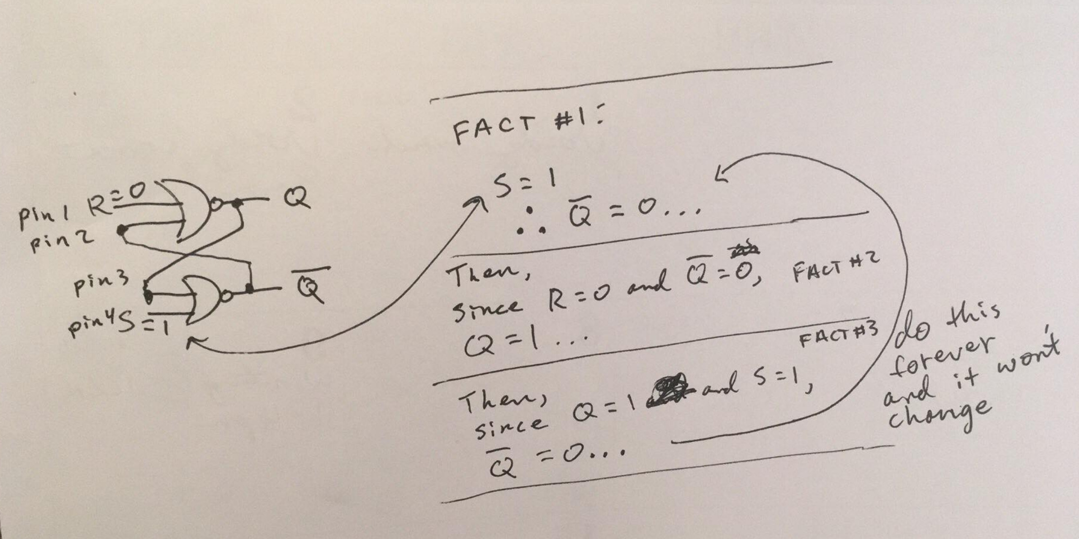
In the diagram, our goal is to produce the set effect.
Start by noticing pins 1 & 4 where R is set to 0 and S is set to 1. Disregard the values of Q and ~Q because we cannot affect them directly, (because they are outputs of the system, not inputs).
Take into account the statement, “NOR will output a 0 if either input is a 1,
otherwise it will output 0”. Then see that S = 1, therefore the NOR
statement applies (at least one input is 1, so NOR outputs 0). Therefore, the
output ~Q must equal 0!
That’s fact #1. S = 1, therefore ~Q = 0.
From that we can continue to run values through the loop.
Since, R is 0 and the other gate input (~Q) is also 0, we can use the definition
of a NOR to conclude that it’s impossible for the output to be a 0. Q must
equal 1 because both inputs are 0.
That’s fact #2. R = 0 and ~Q = 0, therefore Q = 1.
Now for the last step, looking back at the bottom gate again, we already know
that S = 1 — that’s a given. But now we know that Q = 1 as well.
This doesn’t really change anything because the NOR gate already has
an input of 1, from S. In fact, this step wasn’t necessary at all, but
from here we can trace ~Q = 0 back to Fact #1. The process will repeat
in this loop forever.
This looping forever idea is our stable state. We’ve settled on a final
state! Q = 1 and ~Q = 0, just like the truth table. We’ve acheived
the set effect.
Proving the other conditions
To prove that the other effects occur appropriately, just rinse and repeat the process above. Draw the gates. Pick values for R and S. Then check if the output matches the truth table. If it does, then the full functionality of our spec is there. The latch can persist state correctly.
However, you might find the second method easier, as it’s automated.
Code
To double-check our gate design (and to squash any remaining doubters of our latch’s abilities), we can show that this works by describing the hardware in code and running simulations (referred to as testbenches in the hardware description world, or verification if you’re getting fancy).
Intro to Verilog
Before we dive into writing the logic for the SR Latch, let’s look at some basic Verilog code and break it down.
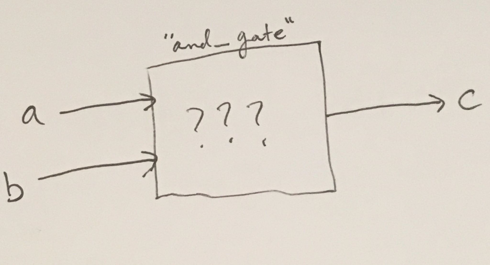
// Here we declare a module named "and_gate" with two inputs and one output.
module and_gate(
    input  wire a, b, // Wires in Verilog are like wires in real life,
    output wire c);   // you can tie them together in any static configuration,
                      // and electrical impulses can propagate in near real-time
                      // without any effort on your part! Just hook them up to
                      // a combinational circuit, such as a lone AND gate,
                      // and the output will always change based on the input.

    // Here we are assigning the wire c to the output of combinational logic:
    // a AND b. The output c will change instantly to adapt to the inputs
    // a and b.
    assign c = a & b;
endmodule
If this idea still seems foreign to you, look at it in this light:
We’ve described a black-box of sorts, called a module. Abstractly, it looks something like this:
But suppose we were an omni-sentient being, and we could peer down into the depths of digital logic with ease… then we would see something like this:
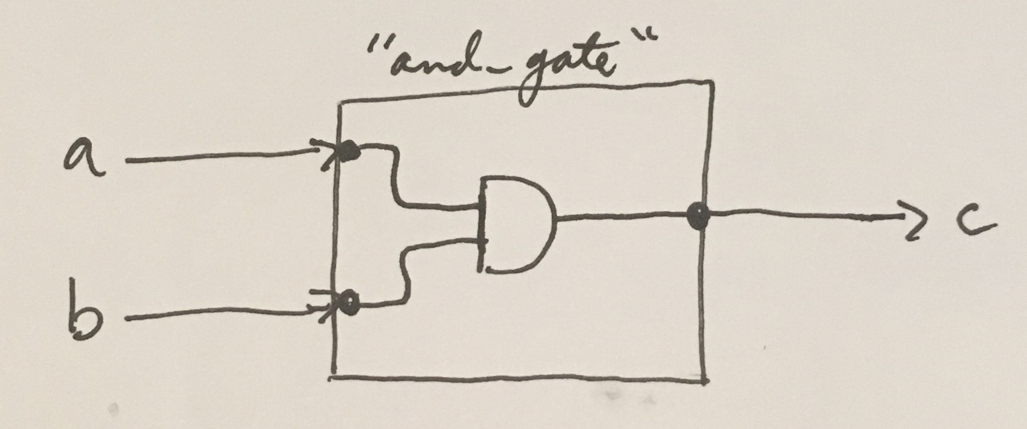
Of course, this internal logic can become much more complicated. That’s where the beauty of it comes in. We can define module after module. And within each module, we can include a submodule, which includes a submodule in itself, and so forth. Eventually, we can abstract our systems sufficiently to create incredibly complex and powerful systems. These systems include CPUs, GPUs, MCUs, ALUs, network switching fabrics, HDMI encoders/decoders, and many, many, more.
for reference:
CPU(Central Processing Unit),
GPU(Graphics Processing Unit),
ALU(Arithmetic Logic Unit),
MCU(Microcontroller Unit)
Creating an SR Latch in Verilog
Hopefully, by now you have a good grasp on how the SR latch functions as a whole and understand the utility of Verilog when it comes to digital logic design. Here we’ll describe the functionality of our SR latch in Verilog, then run some simulations to prove that it functions correctly.
Implementation
// file: sr_latch.v
// Using Verilog to describe our SR Latch
module sr_latch(
    input wire S, R,
    output wire Q, Q_not);

    assign Q     = ~(R | Q_not);
    assign Q_not = ~(S | Q);
endmodule
 Building on what we previously described, here is our `sr_latch` module
rendered as a black-box (with and without seeing the internal logic).
Building on what we previously described, here is our `sr_latch` module
rendered as a black-box (with and without seeing the internal logic).The important takeaway is that the "hardware is the code" and the "code is the hardware". They are both valid descriptions of the same idea, one just happens to be graphical — and the other happens to be code.
Simulation
// file: sr_latch_tb.v
// Using a testbench to simulate our module
`include "sr_latch.v"
module sr_latch_tb;

// create test registers, then instantiate our module
 reg s, r;     // we can modify registers as we please to simulate the inputs
wire q, q_not; // we can't modify these, because they are assigned in our module
sr_latch latch(s, r, q, q_not);

// not a verilog construct,
// just for the testbench
integer x;

initial begin
    // for waveform analysis
    $dumpfile("sr_latch.vcd");
    $dumpvars(s, r, q, q_not);

    // case 1 (latch w/o state)
    s=0; r=0; #1
    $display("s=%b, r=%b ==> q=%b, q_not=%b # should be undefined",
              s, r, q, q_not);

    // case 2 (reset)
    s=0; r=1; #1
    $display("s=%b, r=%b ==> q=%b, q_not=%b # reset, so q=0",
              s, r, q, q_not);

    // case 3 (set)
    s=1; r=0; #1
    $display("s=%b, r=%b ==> q=%b, q_not=%b # set, so q=1",
              s, r, q, q_not);

    // case 4 (latch with state)
    s=0; r=0; #1
    $display("s=%b, r=%b ==> q=%b, q_not=%b # latch, so q=q (keep state)",
              s, r, q, q_not);

    // case 5 (invalid state)
    s=1; r=1; #1
    $display("s=%b, r=%b ==> q=%b, q_not=%b # invalid state, so discount error",
              s, r, q, q_not);
end

endmodule
Simulation Output
$ iverilog sr_latch_tb.v
$ ./a.out
VCD info: dumpfile sr_latch.vcd opened for output.
s=0, r=0 ==> q=x, q_not=x # should be undefined
s=0, r=1 ==> q=0, q_not=1 # reset, so q=0
s=1, r=0 ==> q=1, q_not=0 # set, so q=1
s=0, r=0 ==> q=1, q_not=0 # latch, so q=q (keep state)
s=1, r=1 ==> q=0, q_not=0 # invalid state, so discount error
And it matches our truth table exactly! Our graphical design has met our Verilog specifications.